
Listen to this Post
Introduction:
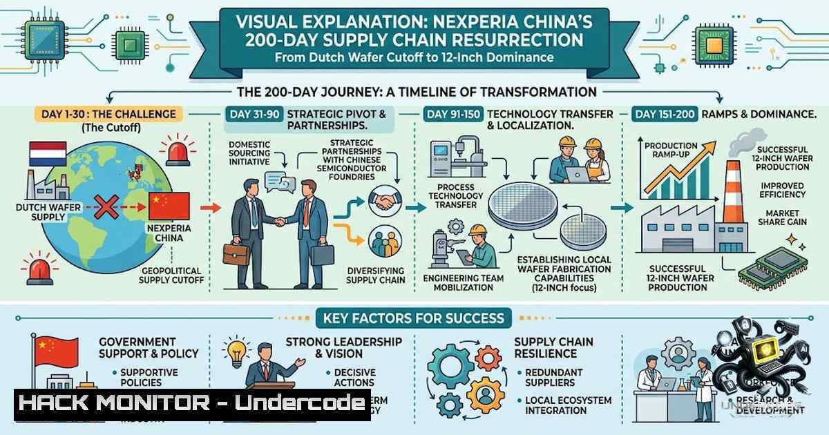
In a dramatic display of supply chain resilience, Nexperia China has executed one of the fastest semiconductor manufacturing turnarounds in recent history. After the Dutch government seized control of Nexperia in September 2025 and halted wafer shipments to its Chinese operations in October, the company’s Chinese subsidiary restructured its entire manufacturing ecosystem from the ground up. Within 200 days, Nexperia China transitioned from being cut off from European wafer supplies to establishing an independent 12-inch power semiconductor platform, delivering over 40 billion chips to more than 1,000 global customers. This case study examines how the company navigated the crisis, the technical implications of its 12-inch wafer breakthrough, and the cybersecurity lessons for semiconductor supply chains worldwide.
Learning Objectives & Secrets:
- Objective 1: Understand the 12-inch wafer advantage – Learn how transitioning from 6-inch and 8-inch wafers to 12-inch (300mm) platforms delivers 2.2–2.4 times more chips per wafer and reduces per-chip costs by up to 50%.
-
Objective 2 Secret Tip: Master supply chain decoupling strategies – Nexperia China’s rapid localization from less than 20% to nearly 100%国产化率 was achieved through simultaneous qualification of domestic wafer suppliers including WingSkySemi (12-inch), Shanghai GAT Semiconductor, and United Nova Technology (8-inch IGBT).
-
Objective 3 Secret Tip: Accelerate product development cycles – The company compressed industry-standard 24–36 month development cycles to just 6–12 months, while production ramp-up time dropped from 12–16 weeks to 4–6 weeks. The secret: parallel engineering across chip structure, process integration, and manufacturing flow optimization on the 12-inch platform.
You Should Know:
- The 12-Inch Wafer Revolution: Cost, Efficiency, and Performance
The shift to 12-inch wafers represents a fundamental manufacturing paradigm change. A 12-inch wafer’s surface area is 2.25 times that of an 8-inch wafer, translating to 2.2–2.4 times more effective chips per wafer. Compared to 5-inch wafers, output increases 5.7-fold; compared to 6-inch, 4-fold. Per-chip costs drop approximately 70% versus 5-inch, 60% versus 6-inch, and 50% versus 8-inch wafers.
Step-by-Step Guide: Calculating Wafer Transition ROI
For semiconductor operations leaders evaluating wafer transitions:
- Calculate die per wafer (DPW): Use the formula DPW ≈ (π × (Wafer Diameter/2)²) / (Die Area) – (π × Wafer Diameter) / (√(2 × Die Area)). For a 300mm wafer versus 200mm, DPW increases by ~2.25×.
-
Factor in yield learning: Nexperia China’s first 12-inch production line achieved 30-day continuous yield stability above 92.7%. Model yield ramp using the standard semiconductor yield learning curve: Y = Y₀ × (cumulative volume)^(-α), where α typically ranges 0.15–0.30.
-
Compute total cost per good die: Include wafer cost, processing steps, test costs, and packaging. Nexperia China’s localized supply chain reduced logistics costs by 15–20% and eliminated cross-border tariffs.
-
Automation impact: Full automation reduced human intervention by over 90%, directly improving yield consistency.
Linux Command Example – Yield Data Analysis:
 Parse wafer sort test data and calculate yield by lot
awk -F',' '{if($3=="PASS") good[$1]++; total[$1]++}
END {for(lot in good) printf "Lot %s: Yield %.2f%%\n", lot, (good[bash]/total[bash])100}' wafer_test_data.csv

Monitor equipment uptime across 12-inch production lines
grep "EQUIPMENT_STATUS" /var/log/semiconductor/fab_logs/.log | \
awk '{print $4}' | sort | uniq -c
2. Supply Chain Resilience: The 200-Day Recovery Timeline
Nexperia China’s recovery offers a masterclass in supply chain crisis management. Key milestones:
- September 30, 2025: Dutch government invokes law to take over Nexperia
- October 26, 2025: Dutch headquarters halts wafer shipments; systems go offline; overseas data becomes inaccessible
- November 2025: Partial relaxation of measures; Nexperia China secures local wafer commitments
- December 2025: Local wafer supply locked in for entire 2026 production
- March 2026: Small-batch 12-inch wafer bipolar discrete production announced
- May 2026: Independent operations system with full decision-making authority completed
- August 2026: Global product launch; 40 billion chips delivered
Step-by-Step Guide: Building an Independent Semiconductor Supply Chain
- Dual-source critical materials: Nexperia China qualified multiple domestic wafer suppliers simultaneously – WingSkySemi for 12-inch (30,000 wafers/month capacity), plus 8-inch IGBT suppliers.
-
Establish independent IT and data infrastructure: When the Dutch headquarters “went offline” and data became inaccessible, the Chinese unit had to rebuild systems. This required:
– Independent ERP and MES (Manufacturing Execution Systems)
– Localized EDA (Electronic Design Automation) toolchains
– Secure data backup and disaster recovery protocols
- Accelerate product qualification: The company’s 19 new products covered over 80% of demand within months.
Windows Command Example – Supply Chain Monitoring:
 Monitor supplier delivery performance
Get-Content -Path "C:\SupplyChain\supplier_delivery.log" | `
Select-String "WingSkySemi" -Context 2,2 | `
ForEach-Object { $_.Line -match "DELIVERED|DELAY" }

Track inventory levels across multiple warehouses
Import-Csv "C:\Inventory\warehouse_stock.csv" | `
Group-Object ProductFamily | `
Select-Object Name, @{N='TotalQty';E={($_.Group | Measure-Object -Property Qty -Sum).Sum}}
3. Semiconductor Supply Chain Cybersecurity Risks
The semiconductor industry faces escalating cyber threats that Nexperia’s crisis inadvertently highlighted. When overseas systems “went offline” and data became inaccessible, it demonstrated how supply chain dependencies create single points of failure – not just from geopolitics but from cyber vulnerabilities.
Key cybersecurity risks in semiconductor manufacturing:
- Compromised vendor accounts providing backdoor entry into fab systems
- Insecure remote maintenance channels exposing tool interfaces
- Legacy OT systems running unsupported operating systems (Windows XP/7) that cannot be patched
- Data leakage from design partners or subcontractors
- Hardware Trojans – a tangible, not theoretical, threat
- Insider misuse of design files and insufficiently secured vendor networks
Step-by-Step Guide: Securing Semiconductor Manufacturing IT/OT
- Inventory all OT assets: Identify every manufacturing tool, controller, and edge device. Pay special attention to “proprietary, unsupported, or end-of-life operating systems”.
-
Implement network segmentation: Isolate OT networks from IT networks. Many semiconductor fabs still rely on “physical isolation” that is eroding as equipment connectivity increases.
-
Enforce zero-trust for third-party access: Third-party involvement in breaches doubled year-over-year to 30%. Eliminate low-barrier workarounds like guest SharePoint access or shared cloud storage.
-
Establish vulnerability reporting processes: Under the Cyber Resilience Act (effective September 11, 2026), manufacturers must report vulnerabilities within 24 hours and provide full notifications within 72 hours.
Linux Command Example – OT Network Security Scanning:
 Scan for exposed industrial protocols on manufacturing subnet
nmap -p 502,102,44818,2222 --open 192.168.100.0/24

Check for legacy SSL/TLS versions on equipment interfaces
sslscan --1o-failed 192.168.100.50:443 | grep -E "SSL|TLS|vulnerable"

Monitor for unauthorized outbound connections from fab tools
sudo tcpdump -i eth0 -1 'dst net ! 192.168.0.0/16 and (tcp or udp)' -c 1000
4. Automotive-Grade Power Semiconductor Leadership
Nexperia holds approximately 40% of the global market for key automotive discrete components. Its automotive-grade power semiconductor products account for more than 30% of the global market. The company ranks:
- No. 1 globally in small-signal diodes and ESD protection devices shipments
- No. 2 globally in automotive-grade Power MOSFETs
- Top 3 globally in logic devices
The 12-inch platform has enabled breakthrough performance: 40V automotive MOSFET on-resistance reduced to 0.48 milliohms – a 50%+ improvement over previous generations; 80V versions at 1.3 milliohms.
Step-by-Step Guide: Automotive Semiconductor Qualification (AEC-Q101)
- Temperature cycling: Test devices from -40°C to +150°C for 1,000+ cycles
- Biased humidity testing: 85°C/85% RH with bias applied for 1,000 hours
- ESD robustness: Human Body Model (HBM) ≥ 2kV; Charged Device Model (CDM) ≥ 500V
- Early failure rate (EFR): < 60 ppm after 48-hour burn-in at 125°C
-
The “China for China” Strategy and Future Outlook
Nexperia China’s strategic framework combines “global automotive-grade standards + rapid localized response”. The company’s国产化率 (localization rate) has climbed from under 20% to nearly 100% for key components. MOSFET and logic IC supply chains are now fully closed-loop within China, with bipolar transistors expected to complete full-stack domestic supply chain closure by end of 2026.
What Undercode Say:
- Key Takeaway 1: Nexperia China’s 200-day recovery demonstrates that semiconductor supply chains can be rebuilt from scratch when geopolitical disruptions occur – but only with coordinated action across wafer sourcing, manufacturing, packaging, and IT infrastructure. The company’s ability to deliver 40 billion chips with “zero quality incidents” during this transition is remarkable.
-
Key Takeaway 2: The 12-inch wafer transition is not merely about cost reduction – it represents a strategic moat. With 12-inch platforms delivering 50% lower per-chip costs and 2.2× higher output, companies still reliant on 6-inch and 8-inch wafers face structural cost disadvantages. Nexperia’s Dutch parent, which lacks 12-inch capabilities in Europe, now competes against its own subsidiary with a technology gap.
Analysis: The Nexperia China case reveals three critical lessons for the global semiconductor industry. First, supply chain concentration creates existential risks – the Dutch government’s seizure and subsequent wafer cutoff triggered a crisis that nearly halted global auto production. Second, technological independence requires parallel investment in manufacturing infrastructure, supply chain partnerships, and IT systems – Nexperia China succeeded because it had already established relationships with domestic wafer suppliers before the crisis escalated. Third, the semiconductor industry’s cybersecurity posture remains dangerously fragmented; as fabs become more connected and third-party dependent, the attack surface expands exponentially. NIST’s ongoing work on semiconductor supply chain traceability and cybersecurity frameworks is essential but must be adopted faster than the current pace of industry implementation.
Prediction:
- +1 Nexperia China will achieve 100% local production for most automotive and industrial chips by Q4 2026, creating a fully independent semiconductor ecosystem that can operate without European wafer inputs. This will accelerate China’s broader semiconductor self-sufficiency goals.
-
+1 The company’s 12-inch platform will enable aggressive pricing in power discrete devices, potentially reshaping global market share dynamics as the cost advantage (50% lower per-chip costs) passes through to customers.
-
-1 The geopolitical schism between Nexperia’s Dutch parent and Chinese subsidiary will not be resolved amicably. Legal proceedings and corporate governance disputes will continue, creating ongoing uncertainty for global customers who rely on Nexperia products.
-
-1 Semiconductor supply chain cyberattacks will increase as geopolitical tensions rise. The Advantest ransomware attack and other incidents demonstrate that testing equipment, supply chain partners, and legacy OT systems are prime targets. Nexperia China’s newly built IT infrastructure, while modern, must be continuously hardened against evolving threats.
-
+1 The 12-inch platform’s performance breakthroughs – particularly the 0.48 mΩ 40V automotive MOSFET – will drive adoption in AI servers (48V bus applications) and next-generation electric vehicles, positioning Nexperia China as a key supplier for high-growth sectors including AI infrastructure, smart vehicles, photovoltaics, and industrial automation.
▶️ Related Video (82% Match):
https://www.youtube.com/watch?v=7gPn_4ja1jU
🎯Let’s Practice For Free:
🎓 Live Courses & Certifications:
Join Undercode Academy for Verified Certifications
🚀 Request a Custom Project:
Secure, high-velocity infrastructure and disruptive technological engineering. Contact our engineering team for high-tier development and proprietary systems:
[email protected]
💎 Smart Architecture | 🛡️ Secure by Design | ⭐ Trusted by Thousands
IT/Security Reporter URL:
Reported By: https://lnkd.in/p/e_HScE7s – Hackers Feeds
Extra Hub: Undercode MoN
Basic Verification: Pass ✅


